Packaging
We offer the highest quality, most economicallypriced static shield packaging available. With 40% light transparency, itallows for easy identification of IC's (integrated circuits) and PCB's (printedcircuit boards). The extremely durable buried metal contruction gives FaradayCage performance needed to effectively shield these componenets against staticcharge.
All the products will packing in anti-staticbag. Ship with ESD antistatic protection.
Outside ESD packing’s lable will use ourcompany’s information: Part Mumber, Brand and Quantity.
We will inspect all the goods before shipment,ensure all the products at good condition and ensure the parts are new originalmatch datasheet.
After all the goods are ensure no problems afterpacking, we will packing safely and send by global express. It exhibitsexcellent puncture and tear resistance along with good seal integrity.
We can offer worldwide express delivery service, such as DHLor FedEx or TNT or UPS or other forwarder for shipment.

Global Shipment by DHL/FedEx/TNT/UPS
Shipping Fees reference DHL/FedEx
1). You can offer your express delivery account for shipment, ifyou haven’t any express account for shipment, we can offer our account inadvance.
2). Use our account for shipment, Shipment charges(Reference DHL/FedEx, Different Countries has different price.)
| Shipment charges: |
(Reference DHL and FedEX) |
| Weight(KG): 0.00kg-1.00kg |
Price(USD$) : USD$60.00 |
| Weight(KG): 1.00kg-2.00kg |
Price(USD$) : USD$80.00 |
* The price of cost is reference with DHL/FedEx. The detail charges, please contact us. Different country the express charges are different.
- Other Shipment Way: SF Express for Asia; Chang-woo special air line for Korea, Aramexfor Middle East countries. Others more shipping way, please contact us.
We also can send the goods to your forwarder or your othersupplier, so that you can send the goods together. It may will save shipmentcharges for you, or may will more convenient for you.
- Shipping Details: Shippinginformation, We need shipping information including Receiver Company Name(Or personal), Receiver Name, Contact Number, Address and Zip Code. Please make sure these information to us, so that we can arrange the shipment faster.
- Delivery time: Deliverytime will need 2-5days to most of country all over the world for DHL/UPS/FEDEX/TNT.
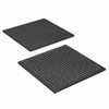
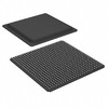
XC6SLX100-2CSG484C Product Details:
"XC6SLX100-2CSG484C: An Overview of Its Versatile Applications, Features, and Manufacturing Process"
XC6SLX100-2CSG484C by Xilinx is a highly integrated Field Programmable Gate Array (FPGA) consisting of digital, mixed-signal, and radio frequency (RF) circuits. This FPGA comes with 338 input/output (I/O) pins and a 484 chip-scale ball grid array (CSBGA) package. This article will introduce XC6SLX100-2CSG484C's unique features, performance parameters, applications, and the intricate manufacturing process.
Highlighting the product's features, XC6SLX100-2CSG484C has a minimum supply voltage of 1.14V and a maximum of 1.26V with an input clock frequency of 550 MHz. It operates at an ambient temperature range between -40°C and 100°C and has a dynamic power consumption of 1.08W at maximum performance. This flexible FPGA is ideal for applications requiring high-speed, low-power consumption, and low latency communication among systems.
This FPGA is versatile and can be used in several electronic devices and industries, including automotive, aerospace, defense, and communication systems. Its high-speed processing capability, low noise emission, and reprogrammability makes it a popular choice for embedded systems, audio and video processing, and network routers. The XC6SLX100-2CSG484C can also be used for prototyping and scientific research in signal processing, computer vision, and machine learning.
Designing and manufacturing an FPGA is a complex process involving several stages. The process starts with chip design, where the overall architecture is designed by engineers. The next stage involves cutting and cleaning the silicon wafer, followed by laser processing to etch the circuit layout. Back grinding is then undertaken to reduce wafer thickness. The chip is then doped, exposed, and vapor deposition is applied before etching to introduce the final features. The finished product undergoes packaging and testing to ensure the correct component quality, reliability, and functionality.
In conclusion, the XC6SLX100-2CSG484C FPGA is a versatile and efficient IC used in several industrial applications. This article highlighted its unique features, performance parameters, and manufacturing process while emphasizing the application scenarios and usage. The article aims to provide technical information to researchers and professionals looking to use or modify this FPGA. Whether designing, analyzing, or researching integrated circuits, the XC6SLX100-2CSG484C is an invaluable tool.