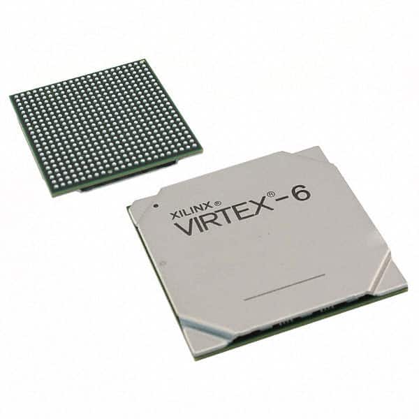
Packaging
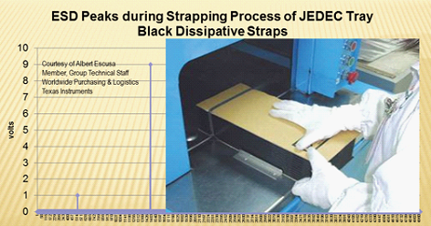
We offer the highest quality, most economicallypriced static shield packaging available. With 40% light transparency, itallows for easy identification of IC's (integrated circuits) and PCB's (printedcircuit boards). The extremely durable buried metal contruction gives FaradayCage performance needed to effectively shield these componenets against staticcharge.
All the products will packing in anti-staticbag. Ship with ESD antistatic protection.
Outside ESD packing’s lable will use ourcompany’s information: Part Mumber, Brand and Quantity.
We will inspect all the goods before shipment,ensure all the products at good condition and ensure the parts are new originalmatch datasheet.
After all the goods are ensure no problems afterpacking, we will packing safely and send by global express. It exhibitsexcellent puncture and tear resistance along with good seal integrity.
We can offer worldwide express delivery service, such as DHLor FedEx or TNT or UPS or other forwarder for shipment.

Global Shipment by DHL/FedEx/TNT/UPS
Shipping Fees reference DHL/FedEx
1). You can offer your express delivery account for shipment, ifyou haven’t any express account for shipment, we can offer our account inadvance.
2). Use our account for shipment, Shipment charges(Reference DHL/FedEx, Different Countries has different price.)
| Shipment charges: |
(Reference DHL and FedEX) |
| Weight(KG): 0.00kg-1.00kg |
Price(USD$) : USD$60.00 |
| Weight(KG): 1.00kg-2.00kg |
Price(USD$) : USD$80.00 |
* The price of cost is reference with DHL/FedEx. The detail charges, please contact us. Different country the express charges are different.
- Other Shipment Way: SF Express for Asia; Chang-woo special air line for Korea, Aramexfor Middle East countries. Others more shipping way, please contact us.
We also can send the goods to your forwarder or your othersupplier, so that you can send the goods together. It may will save shipmentcharges for you, or may will more convenient for you.
- Shipping Details: Shippinginformation, We need shipping information including Receiver Company Name(Or personal), Receiver Name, Contact Number, Address and Zip Code. Please make sure these information to us, so that we can arrange the shipment faster.
- Delivery time: Deliverytime will need 2-5days to most of country all over the world for DHL/UPS/FEDEX/TNT.
CK-V6-ML623-G Product Details:
CK-V6-ML623-G Development Board: A Comprehensive Overview of the Embedded Complex Logic Kit
The CK-V6-ML623-G development board is a powerful tool for embedded complex logic analysis. As one of the most versatile development kits on the market, it offers advanced features and performance parameters that can fulfill the most challenging demands of FPGA and CPLD design and analysis.
In this article, we will provide a deep exploration of CK-V6-ML623-G development board from various perspectives, including product classification, main features, application scenarios, usage, complex manufacturing process, and more.
Product Classification and Main Features
As a comprehensive development kit, the CK-V6-ML623-G board belongs to the embedded complex logic category. It integrates various essential components, such as Gigabit Ethernet, a high-speed FPGA, DDR3 memory, and a compact flash.
The main features of this development board include a 6-layer PCB design, an on-board regulator, and a USB programming interface. Additionally, it has a design that complies with Intel's Avalon Bus protocols. The board is packaged with multiple carrier cards, including TOSA, ROSA, SFP+VCSO, QSFP+, QSFP+VCSO, and more.
Performance Parameters
The CK-V6-ML623-G development board has impressive performance parameters, including an output voltage of 0.95V–1.05V and an operating voltage between 5V and 15V. The maximum voltage is 17V. Furthermore, it has a current range of 0-5A, minimum input voltage of 4.5V and output power of 25W on the development board. It has an efficiency of over 87%, and a temperature range of -40℃ to +125℃.
Application Scenarios and Usage
The CK-V6-ML623-G board has a wide range of application scenarios and usage. It can be used to develop high-speed system designs, say in the telecom industry, and data center applications requiring advanced SERDES solutions. Also, it is incredibly suitable for high-speed communication, wired and wireless infrastructure, and high-end FPGA applications. Some of the electronic devices it is compatible with include memory modules, signal generators, logic analyzers, and more.
Different Types of Integrated Circuits
Integrated circuits are vital components in the development of highly functional electronic devices. There are different types of integrated circuits, including digital, analog, mixed signal, and RF integrated circuits. The CK-V6-ML623-G development board includes digital, analog, and mixed signal ICs.
Complex Manufacturing Process
The CK-V6-ML623-G development board requires a complex manufacturing process, which includes chip design, cutting, cleaning, laser processing, back grinding, doping, exposure, vapor deposition, etching, and testing.
Finished Products
The finished products need to undergo appropriate packaging and testing to ensure component quality. Testing is typically carried out by connecting the CK-V6-ML623-G development board to a different device, such as a logic analyzer, oscilloscope, or other proprietary tools. Additionally, the product needs to be packaged appropriately to avoid damage during transportation.
Conclusion
In conclusion, the CK-V6-ML623-G development board is an excellent tool for FPGA and CPLD design and analysis. We have explained in this article its classification, main features, performance parameters, application scenarios, usage, and manufacturing process. If you are looking for a versatile and advanced development kit, the CK-V6-ML623-G board is your best bet.